LabVIEW Software for Agilent 6645A
LabVIEW Control Software for Agilent 6645A Source meter
2011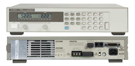
Output Ratings
Output voltage: 0 to 120 V
Output current (40° C): 0 to 1.5 A
Maximum current (50° C/55° C): 1.4 A/1.3 A
Programming Accuracy at 25°C ±5°C
Voltage 0.06% + 51 mV
Current 0.15% + 1.7 mA
Ripple & Noise (20 Hz - 20 MHz)
Voltage rms: 700 µV
Voltage peak-to-peak: 7 mV
Current rms: 1 mA
The Agilent high performance DC power supplies offer speed and accuracy for test optimization. The single output, 200 W, GPIB 6641A-6645A provide fast, low-noise outputs; analog control of output voltage and current; fan-speed control to minimize acoustic noise; as well as parallel and series connections of multiple units.
The Agilent 180W, GPIB, single output 6645A is a versatile programmable supply designed to maximize test throughput during design verification or on the production line, and is fully programmable to help reduce test time through a variety of automated capabilities.
A basic LabVIEW library application program was obtained from Agilent – the HP66xxA. This had basic functions to activate the source-meter and prevent overvoltage.
It was coupled to a PC running LabVIEW 2010 via a GPIB to USB interface cable, configured using the Measurement and Automation Explorer (MAX) to operate from one of the COM ports.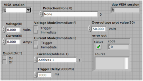
Figure 1: Front Panel of Base Application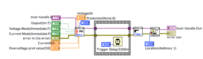
Figure 2: Block Diagram for Base Application
The HP66xxA Application 1.vi was modified to include the Read Measurement vi. This was wired into the VISA and Error lines between the trigger.vi and save-recall-setup.vi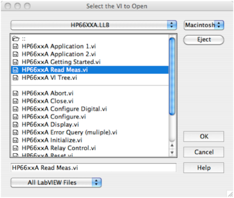
Figure 3: Menu used to add VI components to main application
Additionally, the application was modified with a while loop to provide continuous operation of the application and an enlarged PSU activation control was inserted and the original PSU on-off switch was replaced..
Chart displays indicating the output voltage and current, related to the input settings, and data from both current and voltage lines were combine signals element and a write_to_data_file.vi was included to allow for data collection.
The loop stop function was connected via a NOT gate to invert the signal from the stop loop – this incorporated a safety feature where the PSU was switched off when the application was terminated.
The charts were set to reset to zero each time they were called – re-zeroing the displays, using an option form the VI preferences panel. The delay trigger was reduced from 5000ms to 100ms and the overvoltage value was set as 110V. Both set as default
Finally, the GUI was modified as shown to make the functions more accessible. Error displays were grouped into one area, input settings were grouped into another area and output settings into a third area. Unused functions were grouped to a location in the centre of the screen and the VISA selection functions were located at the top of the screen, along with the PSU on/off function and the application terminate function.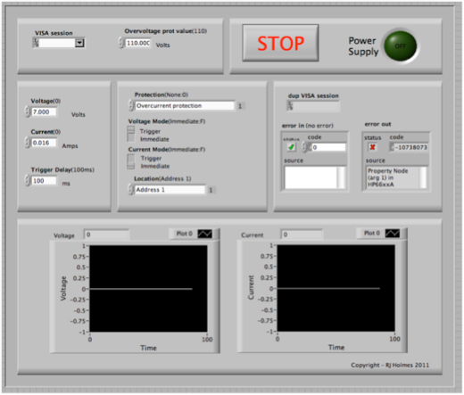
Figure 4: GUI of Prototype Application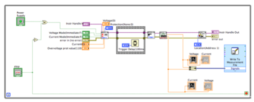
Figure 5: Block diagram of Prototype Application
The system was tested to ensure output voltage and current matched the desired settings, and that the safety feature activated correctly.